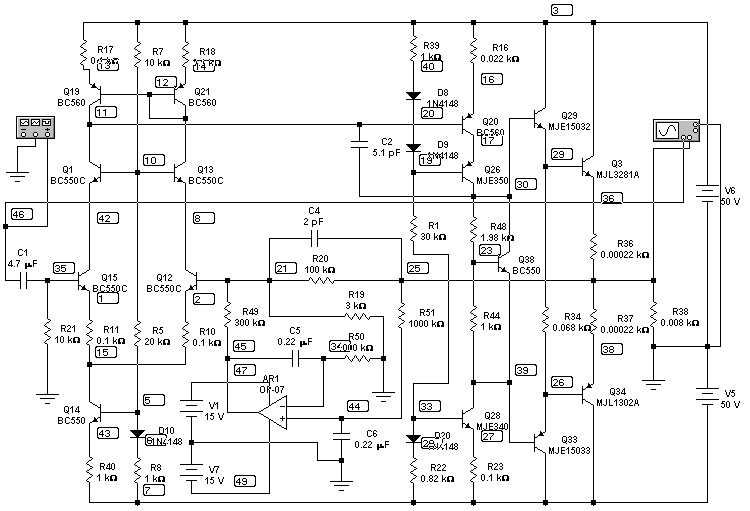
The influence of schematics on power amplifier parameters
The article
"Transistor power amplifier schematics
" describes some solutions used in transistor amplifiers. This article discusses how
technical parameters of an amplifier change with some more complex modifications that are
brought into the basic schematics.
All schematics are simulated with Electronics WorkBench (EWB) and are not for mechanical
implementation in reality. In all amps the same transistors are used and the same quiescent
currents in similar stages (if possible).
What happens when the output stage quiescent bias current is changed is described in:
"The influence of
quiescent bias current of the output stage on the amplifier parameters
".
EWB does a "small-signal distortion analysis" of the circuit, but I don't know how
"small-signal" amplitude is determined, so the absolute values of the second and third
harmonics graphs should be treated as qualitative results.
Special article is about calculations needed for designing Your amplifier:
"The example of amplifier design
calculations".
One shouldn't think that having no comp and SPICE simulation programs like EWB nothing
can be done in electronics. Using engineering calculator I can make DC calculations
of an amp in half an hour, without calculator - in 40 minutes but with less accuracy
(though EWB does it in milliseconds).
All schematics use those transistors, SPICE models of which I have, but such transistors
can be used in real projects, though many other BJT's can be used. As a matter of fact
using "the right" transistors can give a lot. For instance the old scheme with new transistors
can have better characteristics, using transistors with higher transition frequencies can
make amp more stable (and less stable too!) and so on, but I can not cower all questions.
As I can not cover all questions, the same type of output stage on complementary two stage
emitter-folower (Darlington) is shown everywhere, though triples and feedback followers are posiible.
Triples are almost not used now because in old times power transistors with H21e=5-10
were possible and those used here have H21e more than 50. Using complementary feedback
output gives lower distortions, lower saturation voltages though You can not put the two
transistors of a pair on the same heat sink without insulation substrate but this is not
our theme.
All schemes are non-inverting, inverting amps are not considered here, though such amps
have some advantages.
All schemes have DC servo, though it's use is not justified in simple schemes just
because of its cost.
For biassing output stage the same voltage source ("transistor Zener diode") is used,
only resistor with selected value is used instead of potentiometer (which should be used
in real devices). Output transistors quiescent bias current is the same (about 150 mA).
Some of these schematics are relatively unstable (generate on some types of signals),
but these are virtual schematics and so it is not so bad: the task of gaining stability
has to be solved when You design your schematics on concrete transistors. Still I used
frequency compensation capacitors and resistors to achieve maximum stability and provide
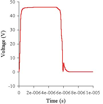
absence of generation. The transient is obtained by making 100 kHz 1V meander input signal.
Every subsequent scheme is a result of evolution of the previous one or some of the previous.
For obviousness amplification factor of all schemes with negative feedback (NFB) is 100/3+1=34.33.
The power supply voltages are +_50V everywhere.
Sometimes pictures of function generator or oscilloscope are present on schematic diagrams:
I simply had no time to remove them. The images of names and values of components are
shown as they are generated by different versions of EWB, so they can differ on some
diagrams on other pages. The numbers of elements are not in order, some numbers are
omitted, but to make proper a dozen of schematic diagrams I had to spent an unpaid week
which I didn't have.
I don't consider the simple schemes without differential stage because they are obsolete
and their inability to produce enough power so the first scheme will be:
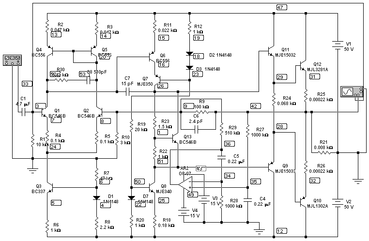
generic schematics with a bootstrap
To begin with, let us examine the old scheme with a bootstrap, which is used by nobody now
(but very good relatively modern integrated circuit TDA7294 uses it!)
With the resistor values shown the first (differential) stage quiescent current is 3.98 mA,
second (voltage amplifier) stage - 16.2 mA, output transistors quiescent current is
114 mA. The first stage current is slightly more than usual in such schemes (1-2 mA),
the second stage current is a bit lower than that in the following schemes. I simply had no
patience to make it the same.
The output stage of emitter follower has lower quiescent current than that in the
following schemes but when I tried to make it 150 mA EWB V5.0 showed "general error"
and I had no V5.12 at that time.
The scheme differs from the old ones by small input pair degeneration emitter resistors
and such resistor in the emitter circuit of Q15 - the voltage amplifier of the second stage.
Without such resistors the amplification factor without NFB at low frequency (1 kHz)would be
higher and low frequency distortions - lower.
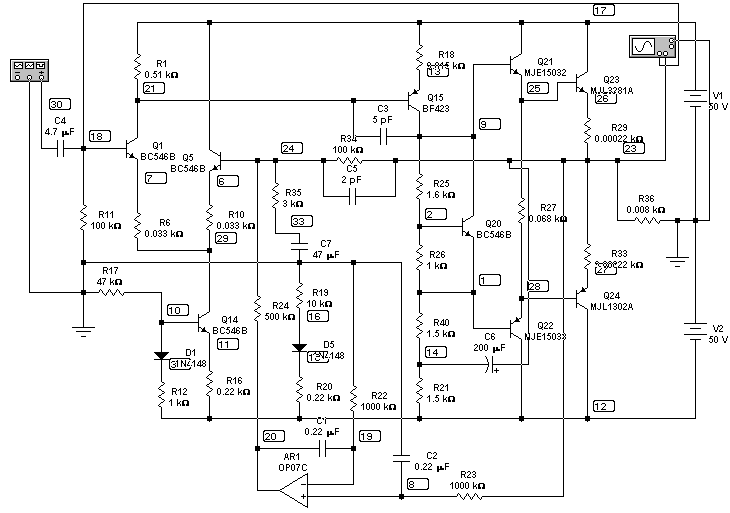
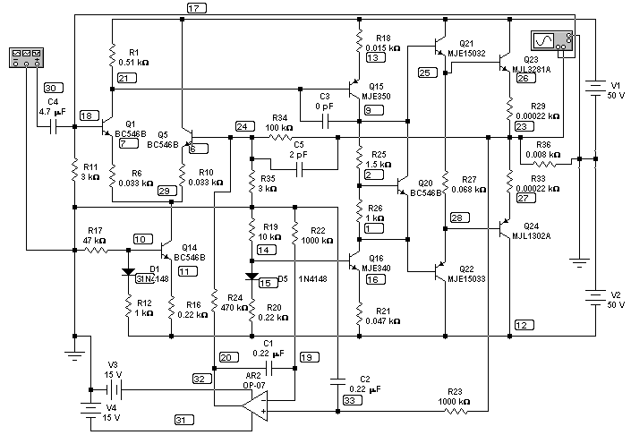
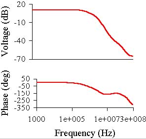
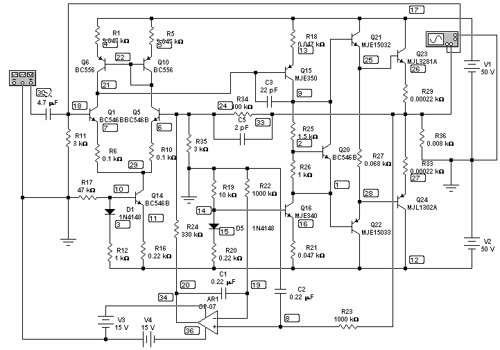
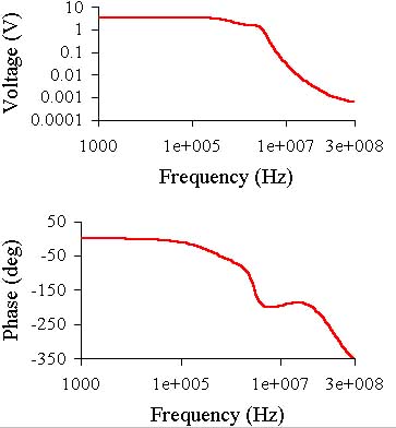
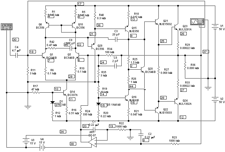
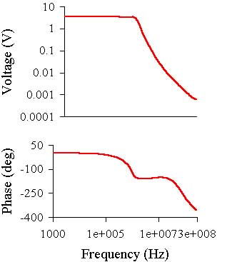
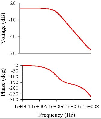
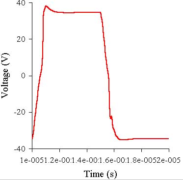
The gain and phase versus frequency graphs and square wave at the output are shown below:
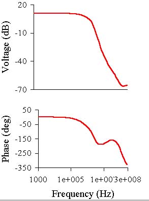
Blue - input signal, red - output (and further always so). Below only "red" graph is shown because
the input is always the same.
R.m.s. sine voltage during frequency analysis is 10 mV, amplitude of square impulse is 1 V,
it's so in other cases.
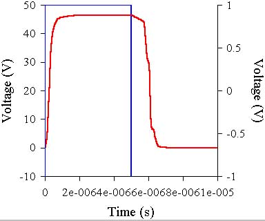
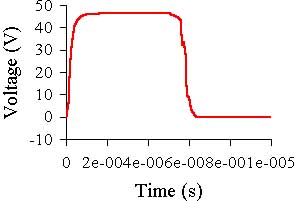
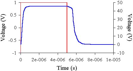
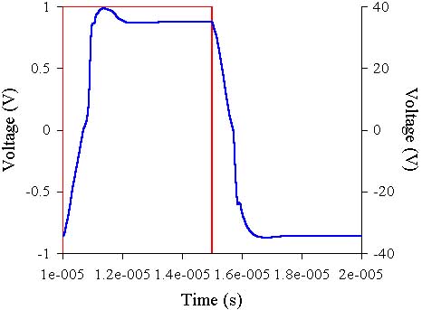
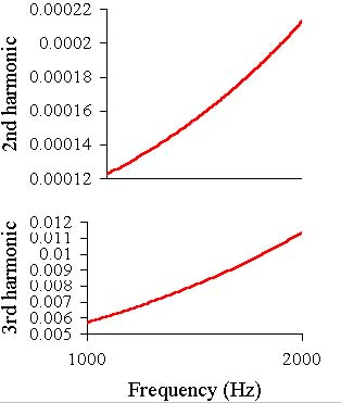
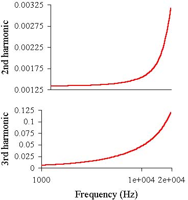
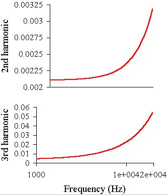
And at last what it is all for: second and third distortion harmonics graphs at 1 kHz - 20 kHz:
Strange nature of the second harmonic - it descends with frequency growth - must not
confuse: after 20 kHz it begins to grow. At the starting frequency (1 kHz) the value
of both harmonics is about 0.05.
The amp is absolutely stable (at resistive loads). This can be achieved with two compensation
capacitors: C3 and the lead compensation -C5. Usually only the first is present but using both or
lead compensation makes it possible to make higher the open loop gain at sound frequencies.
But obtaining of optimum compensation is not our task now.
And in the end here are the DC operating point (voltages in all nodes of the scheme, which are
shown as numbers in rectangles. Using these voltages humanoid knowing Ohm's law can determine
currents in all branches.
Node Voltage
1 -1.1326
2 -0.30848
3 -48.982
6 -1.282
7 -1.2801
8 -0.0014617
9 1.1064
10 -48.369
11 -49.125
12 -50
13 49.753
14 -25.566
15 -48.939
16 -48.226
17 50
18 -0.54715
19 -0.0014
20 -0.65661
21 49.032
22 0
23 0.00073826
24 -0.55
25 0.56519
26 0.025777
27 -0.024279
28 -0.6288
29 0
30 0
33 -0.55
amplifier with current source voltage amplifier stage (VAS)
In comparison with the previous scheme this one provides lower THD at higher amplitudes
and higher gain, that makes it possible to increase the feedback factor and correspondingly
decrease THD.
Do not be afraid of the 3 kOhm resistor at the input (R11) - this is done for the easier balance
of the amplifier. If th DC servo is not used a capacitor should be put between R35 and ground
and input resistor R11 should be equal to R34=100k.
With the resistor values shown the first (differential) stage quiescent current is 3.98 mA,
second (voltage amplifier) stage - 23.6 mA, output transistors quiescent current is
140.5 mA.
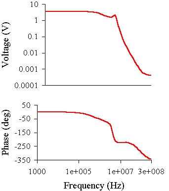
The gain and phase versus frequency graphs and 100 kHz square wave at the output are shown
below:
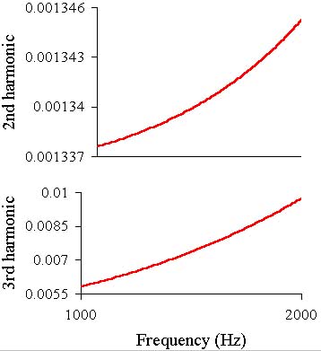
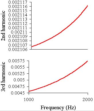
Then the second and third harmonics graphs in the 1 kHz - 20 kHz range.
The scheme is stable, only one capacitor of the lead correction can be used.
The level of the third harmonic at low frequency is almost 10 times lower than in the previous
case, and this is achieved by introduction of a single transistor: Q16.
And nodes voltages at last:
Node Voltage
1 -1.1451
2 -0.29493
3 -48.982
6 -0.75934
7 -0.75158
9 1.1191
10 -48.369
11 -49.125
12 -50
13 49.646
14 -48.271
15 -48.98
16 -48.89
17 50
18 -0.017185
19 -0.00078211
20 -2.2747
21 48.984
23 -4.9568e-006
24 -0.028686
25 0.57705
26 0.030909
27 -0.030919
28 -0.64052
29 -0.82092
30 0
31 -15
32 15
33 -0.00078697
Amplifier with current mirror first stage
In comparison with the previous scheme this one provides
higher open loop gain, that makes it possible to increase the feedback factor and
correspondingly decrease THD.
With the resistor values shown the first stage quiescent current is 3.98 mA,
second (voltage amplifier) stage - 23.57 mA, output transistors quiescent current is
141.5 mA. That is almost the same as in the previous case.
The gain and phase versus frequency graphs and 100 kHz square wave at the output are shown
below (the output signal here is blue):
Then the second and third harmonics graphs in the 1 kHz - 20 kHz band.
The amplifier is stable but the frequency compensation is provided by a rather large
capacitor C3 (larger than in previous case).
The small signal distortion level is approximately the same as in the previous case,
but if the resistor values and currents are optimized the amp shows lower distortions at
low frequencies. Better results can be achieved if a higher H21e transistor is used as Q15.
And nodes voltages at last:
Node Voltage
1 -1.1451
2 -0.29492
3 -48.982
4 49.909
5 49.91
6 -0.75979
7 -0.75016
8 -0.0007853
9 1.1191
10 -48.369
11 -49.125
12 -50
13 48.892
14 -48.271
15 -48.98
16 -48.89
17 50
18 -0.016689
19 -0.00078209
20 -1.4505
21 48.229
22 49.179
24 -0.027926
25 0.57706
26 0.03091
27 -0.030917
28 -0.64052
29 -0.95334
30 0
33 -3.272e-006
34 15
36 -15
amp with emitter-follower in the second stage
Only one more transistor (Q28) and a resistor is used:
With the resistor values shown the first stage quiescent current is 2.38 mA,
second (voltage amplifier) stage - 21.76 mA, output transistors quiescent current is
140.45 mA.
The gain and phase versus frequency graphs and 100 kHz square wave at the output are shown
below (the output signal here is blue):
The stability is achieved only with the use of new RC circuit (R24C8), but still the square
impulse shows small pip after the front. Such frequency compensation is usual in the three
stage voltage amplifiers but here no simple solution could be found.
Then the second and third harmonics graphs in the 1 kHz - 20 kHz range.
The distortions level is much lower than in the previous case and it is strongly dependent from
frequency. So to see the distortions at low frequency the graphs are shown in the 1-2 kHz
range. As one can see the simple innovation gave outstanding result. Although if in the
previous amp better H21e transistors than MJE340-350 were used the result would not be as
radical.
We have to pay for new emitter-follower introduction by stability, but nothing could be done.
The obtained result is explained by substantial increase of the first stage gain because it
works with higher load resistance. Thus the gain begins to decrease at lower frequency which
lays within the sound frequency band (20 Hz - 20 kHz) which is not very good. So at 20 kHz
the third harmonic is not much less than before. So if higher frequency transistors can not
be used the gain can even be made lower using local feedbacks. The low frequency distortions
will be higher but they will begin to grow at higher frequencies.
And nodes voltages at last:
Node Voltage
2 -0.29492
3 -48.981
4 49.945
5 49.945
6 -0.72908
7 -0.72783
8 -0.0007829
9 1.1191
10 -48.368
11 -48.785
12 -50
13 48.892
14 -48.271
15 -48.98
16 -48.89
17 50
18 -0.009939
19 -0.00078207
20 -0.26725
21 47.478
22 49.227
24 -0.011723
25 0.57706
26 0.030913
27 -0.030915
28 -0.64051
29 -0.84706
30 0
34 15
36 48.229
37 -8.5105e-007
38 -15
44 -1.1451
45 47.478
amp with cascode in the second stage
Cascode gives better slew rate not changing the gain. But it makes it possible to use
low voltage high-"beta" transistor as the first in the pair (Q6) thus making it's input
resistance and the first stage gain higher.
With the resistor values shown the first stage quiescent current is 2.38 mA,
second (voltage amplifier) stage - 24.2 mA, output transistors quiescent current is
149 mA. That is almost the same as in the previous case.
The gain and phase versus frequency graphs and 100 kHz square wave at the output are shown
below:
The stability is achieved only with the use of new compensation circuit in the first stage,
but still the square impulse shows a all pip after the front.
Then the second and third harmonics graphs in the 1 kHz - 20 kHz band:
As it can be seen the level of the second and third harmonics is rather low at the low
frequencies, but it is higher than in the previous case and at 20 kHz it is the same, which
means that the open loop gain begins to decrease at higher frequency and a slightly lower
open loop gain at low frequency. From the square impulse "oscillogram" its hard to see
the slew rate growth, but it can be twice as high as in the previous amp.
Nodes voltages:
Node Voltage
1 -0.29683
3 -0.033838
4 -47.812
5 -47.618
6 -47.201
7 -0.75237
8 -0.76039
9 -0.043867
12 -50
13 49.946
14 49.946
15 49.468
16 44.907
18 44.945
19 45.649
20 49.229
22 -45.74
23 44.242
24 -0.87498
25 -45.66
26 1.1232
27 0
28 -0.64385
29 0.58087
31 0.032786
32 -0.032812
33 0
34 -0.00078219
35 -0.00079474
36 -6.1137
42 -1.2808e-005
43 15
47 50
49 -15
50 -45.038
51 -1.1487
52 48.67
53 48.67
amp with cascodes both stages
Cascode gives better slew rate not changing the gain. Such solution is rarely used in the first
stage, because it brings complication but with little gain: the input stage works in a small
signal mode. But in that way we can use low voltage low noise transistors if we have no
BC546-556 type. The Q19, Q21 can be general purpose transistors.
With the resistor values shown the first stage quiescent current is 3,2 mA
second (voltage amplifier) stage - 24.2 mA, output transistors quiescent current is
148 mA. That is almost the same as in the previous case except the first stage.
The gain and phase versus frequency graphs and 100 kHz square wave at the output are shown
below:
The amp is more stable than the two previous ones. The C2 capacitor is small, but
still the square impulse shows a pip after the front.
Then the second and third harmonics graphs in 1-20 kHz and 1-2 kHz bands:
As can be seen the second and third harmonics levels are about the same as as in previous case
at low frequencies, and at 20 kHz they are better than in all described schematics. This is because of the wider open loop frequency range.
The square impulse shows higher slew rate of th amp.
The nodes voltages:
Node Voltage
1 -0.75686
2 -0.76467
3 50
5 -46.129
6 -46.805
7 -50
8 17.198
10 17.92
11 48.668
12 49.119
13 49.844
14 49.845
15 -0.92123
16 49.467
17 46.344
19 45.68
20 46.351
21 -0.040368
23 -0.43279
25 -7.0692e-006
26 -0.64332
27 -47.583
28 -47.631
29 0.58028
30 1.1225
33 -46.962
34 -0.00078213
35 -0.031105
36 0.032493
38 -0.032507
39 -1.1482
40 47.023
41 0
42 17.197
43 -46.783
44 -0.00078906
45 -3.3071
46 0
47 15
49 -15
And in conclusion it must be mentioned that the hybrid schematics with emitter-follower and
cascode in the second stage is possible, but I do not examine it here.
The second part is about symmetrical schematics. The article is divided in two parts simply
to make each part smaller: this part is still 500 kB large.
The second part